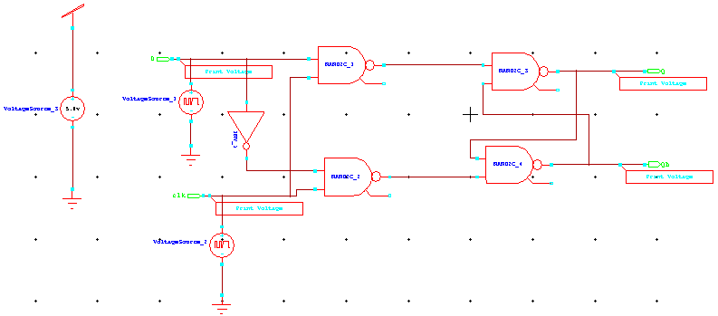
Design of CMOS Flip-Flops (SR, D, JK)


Design of CMOS Flip-Flops (SR, D, JK)

A flip-flop or latch is a circuit with two stable states, used to store state information. It is the basic storage element in sequential logic and a fundamental building block in digital electronics systems, including computers and communication devices.

Flip-flops and latches act as data storage elements for states, pulse counting, and synchronization of variably-timed input signals to a reference clock. Flip-flops can be transparent/opaque (latches) or clocked (synchronous, edge-triggered). Latches are level-sensitive, while flip-flops are edge-sensitive.

In sequential logic, the output depends on current inputs and previous states. Fig.1 shows a sequential circuit combining a combinational block and a memory element.
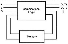
Sequential circuit showing combinational logic block connected to memory element
Fig.1: Sequential circuit consisting of a combinational logic block and a memory
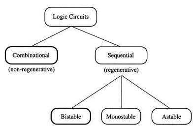
Classification of logic circuits based on temporal behavior
Fig.2: Classification of logic circuits based on temporal behaviour

SR Flip-Flop

The SR latch can be implemented using two NAND gates. The circuit changes state when the Set (S) or Reset (R) input is pulled low. A NAND-based SR latch responds to active-low signals. The truth table and gate-level schematic are shown in Fig.3.
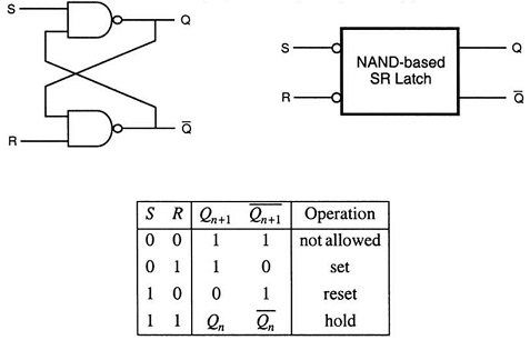
SR latch circuit diagram with block diagram and truth table
Fig.3: Circuit, Block Diagram & Truth Table of SR Latch
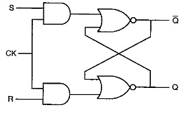
SR flip-flop circuit implementation
Fig.4: Circuit of SR Flip-Flop
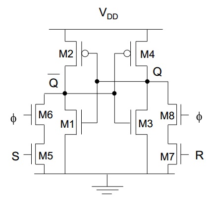
CMOS implementation of SR flip-flop
Fig.5: Circuit of CMOS SR Flip-Flop
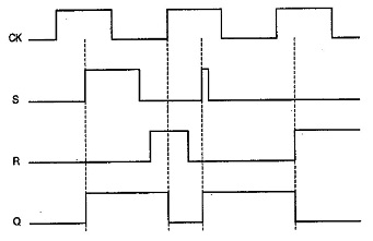
Timing diagram waveform of CMOS SR flip-flop
Fig.6: Timing diagram of CMOS SR Flip-Flop

JK Flip-Flop

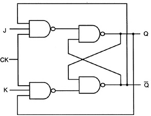
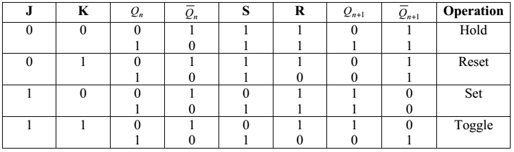
The JK latch solves the "not allowed" input problem of SR latches by using feedback from outputs to inputs. Fig.7 shows an all-NAND JK latch with active-high inputs. J and K correspond to Set and Reset of an SR latch. If both inputs are 1 during the active clock, the latch toggles its state. Table.1 summarizes the JK flip-flop operation.
JK flip-flop NAND gate implementation
Fig.7: NAND implementation of the JK Flip-Flop
Truth table of JK flip-flop
Table.1: Truth Table of the JK Flip-Flop
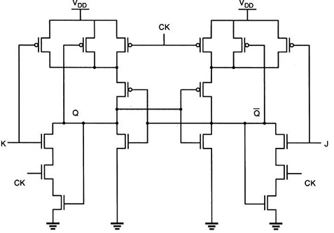
CMOS implementation of JK flip-flop circuit
Fig.8: Circuit of CMOS JK Flip-Flop

D Flip-Flop

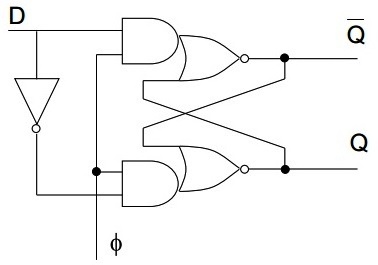
The D-latch stores a single logic level and acts as a 1-bit register. It has input D and outputs Q and Q’. It is implemented using a NOR-based SR latch: D connects to S and D’ to R through an inverter. When CLK is high, D is transmitted to Q; when CLK is low, the previous state is retained.
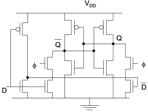
NOR gate implementation of D flip-flop
Fig.9: NOR implementation of the D Flip-Flop
CMOS D flip-flop circuit design
Fig.10: Circuit of CMOS D Flip-Flop

Circuits / Block Diagram using S-Edit
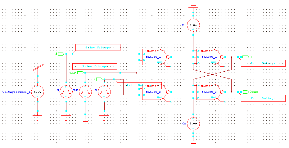
CMOS SR flip-flop schematic using S-Edit
Fig.11: CMOS SR Flip-Flop using S-Edit
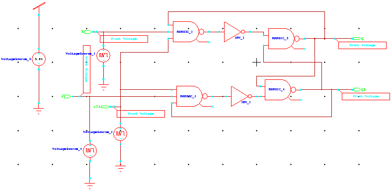
CMOS JK flip-flop schematic using S-Edit
Fig.12: CMOS JK Flip-Flop using S-Edit
CMOS D flip-flop schematic using S-Edit
Fig.13: CMOS D Flip-Flop using S-Edit

Programming (SPICE Command)

Extract SPICE code using T-Edit.

Graphs (W-Edit)

Simulate schematics and generate waveforms using W-Edit.

Conclusions

The transient response of SR, JK, and D Flip-Flops was studied using CMOS logic. Waveforms were obtained using W-Edit, and SPICE code was extracted using T-Edit. Observed waveforms match theoretical truth tables, validating the designs.


Further Reading

  1. Introduction to Tanner EDA Tools
  2. CMOS Logic Gates: Inverter, NAND, and NOR
  3. EDA Tools and VHDL for VLSI Design
  4. Layout of CMOS Inverter
  5. Standard Cell Design in VLSI
  6. Design of CMOS XOR/XNOR Gates
  7. Design of CMOS Full Adder
  8. Design of 8-bit Synchronous Counter
  9. Design of 8-bit Bi-Directional Register
  10. Design of a 12-bit CPU with Basic Instructions
  11. VHDL Logical Function & CMOS Inverter
  12. CMOS Layout Color Codes - IC Design Guide


Contact Us

Name

Email *

Message *

Popular Posts

UGC NET Electronic Science Previous Year Question Papers with Solutions

Home / Engineering & Other Exams / UGC NET 2026 PYQ ⬇️ Download Papers and Solutions 📋 Exam Pattern 💡 Preparation Tips ❓ FAQs 📊 Exam Highlights: Electronic Science (88) Feature Details Junior Research Fellowship (JRF) ₹37,000 + HRA per month Eligibility M.Sc/M.Tech in Electronics (55%) Validity of Certificate JRF (3 Years) | Lectureship (Lifetime) 📥 Download UGC NET Electronics PDFs Complete collection of previous year question papers, answer keys and explanations for Subject Code 88. Start Downloading 📂 View All Question Papers June 2025 - Question Paper Download PDF June 2025 - Solved Paper + Explanation ...

MUSIC Algorithm Explained (with MATLAB + Simulator)

Practical Implementation of the MUSIC Algorithm The focus is on how the algorithm works computationally , not just theory, and it explains the denominator (a H E n E n H a) mathematically and intuitively. 1. Introduction The MUSIC (Multiple Signal Classification) algorithm is a high-resolution method used in signal processing and array processing to estimate the Direction of Arrival (DOA) of signals received by a sensor array. Unlike classical beamforming methods, MUSIC uses eigenvector decomposition of the covariance matrix to separate the signal subspace and noise subspace , allowing it to achieve much higher angular resolution. In practical implementations, MUSIC works by: Simulating or collecting array signals Computing the covariance matrix Performing eigenvalue decomposition Separating signal and noise subspaces Scanning possible angles using a steering vector Constructing a pseudo-spectrum where peaks indicate signal directions 2. Signal Mo...

BER vs SNR for M-ary QAM, M-ary PSK, QPSK, BPSK, ...(MATLAB Code + Simulator)

Bit Error Rate (BER) & SNR Guide Analyze communication system performance with our interactive simulators and MATLAB tools. 📘 Theory 🧮 Simulators 💻 MATLAB Code 📚 Resources BER Definition SNR Formula BER Calculator MATLAB Comparison 📂 Explore M-ary QAM, PSK, and QPSK Topics ▼ 🧮 Constellation Simulator: M-ary QAM 🧮 Constellation Simulator: M-ary PSK 🧮 BER calculation for ASK, FSK, and PSK 🧮 Approaches to BER vs SNR Calculation What is Bit Error Rate (BER)? The BER indicates how many corrupted bits are received compared to the total number of bits sent. It is the primary figur...

MATLAB Code for ASK, FSK, and PSK (with Online Simulator)

MATLAB Code for ASK, FSK, and PSK Comprehensive implementation of digital modulation and demodulation techniques with simulation results. 📘 Theory 📡 ASK Code 📶 FSK Code 🎚️ PSK Code 🕹️ Simulator 📚 Further Reading Amplitude Shift Frequency Shift Phase Shift Live Simulator ASK, FSK & PSK HomePage MATLAB Code MATLAB Code for ASK Modulation and Demodulation COPY % The code is written by SalimWireless.Com clc; clear all; close all; % Parameters Tb = 1; fc = 10; N_bits = 10; Fs = 100 * fc; Ts = 1/Fs; samples_per_bit = Fs * Tb; rng(10); binar...

PSD Calculation with FFT: MATLAB Tutorial for Signal Analysis

  Implementation Steps 1. FFT Computes the Frequency Content of a Signal FFT converts a time-domain signal to the frequency domain. If: The signal is sampled at rate $f_s$ You compute an $N_{\text{FFT}}$-point FFT Then each FFT bin corresponds to a frequency resolution of: $$\Delta f = \frac{f_s}{N_{\text{FFT}}}$$ So the FFT gives you accurate frequency content, assuming the signal is stationary and adequately sampled (Nyquist criterion met).  2. Magnitude Squared Gives Power (Not Amplitude) $$P[k] = |X[k]|^2$$ This gives power at each frequency bin, not just amplitude. It represents how much energy is present at each frequency. It's a key step for PSD.  3. Normalization Makes the PSD Physically Meaningful The equation: $$\text{PSD}[k] = \frac{|X[k]|^2}{N_{\text{FFT}} \cdot f_s \cdot U}$$ is derived from first principles and ensures that the u...

MATLAB code for BER vs SNR for M-QAM, M-PSK, QPSK, BPSK (with Simulation)

🧮 MATLAB Code for BPSK, M-ary PSK, and M-ary QAM Together 🧮 MATLAB Code for M-ary QAM 🧮 MATLAB Code for M-ary PSK 📚 Further Reading MATLAB Script for BER vs. SNR for M-QAM, M-PSK, QPSK, BPSK % Written by Salim Wireless clc; clear; close all; snr_db = -5:2:25; psk_orders = [2, 4, 8, 16, 32]; qam_orders = [4, 16, 64, 256]; ber_psk_results = zeros(length(psk_orders), length(snr_db)); ber_qam_results = zeros(length(qam_orders), length(snr_db)); for i = 1:length(psk_orders) ber_psk_results(i, :) = berawgn(snr_db, 'psk', psk_orders(i), 'nondiff'); end for i = 1:length(qam_orders) ber_qam_results(i, :) = berawgn(snr_db, 'qam', qam_orders(i)); end figure; semilogy(snr_db, ber_psk_results(1, :), 'o-', 'LineWidth', 1.5, 'DisplayName', 'BPSK'); hold on; for i = 2:length(psk_orders) semilogy(snr_db, ber_psk_results(i, :), 'o-', 'DisplayName', sprintf('%d-PSK', psk_or...

Constellation Diagrams of ASK, PSK, and FSK (with MATLAB Code + Simulator)

Constellation Diagrams: ASK, FSK, and PSK Comprehensive guide to signal space representation, including interactive simulators and MATLAB implementations. 📘 Overview 🧮 Simulator ⚖️ Theory 📈 Q-function 📚 Resources BASK Modulation Transmits one of two signals: 0 or $\sqrt{E_b}$, representing binary 0 and 1. Simple but sensitive to noise. BFSK Modulation Transmits one of two signals: $\sqrt{E_b}$ on the Y-axis or $\sqrt{E_b}$ on the X-axis. These are orthogonal signals. BPSK Modulation Transmits $+\sqrt{E_b}$ or $-\sqrt{E_b}$ (antipodal signaling). Most efficient binary scheme. ...

OFDM Symbols and Subcarriers Explained

This article explains how OFDM (Orthogonal Frequency Division Multiplexing) symbols and subcarriers work. It covers modulation, mapping symbols to subcarriers, subcarrier frequency spacing, IFFT synthesis, cyclic prefix, and transmission. Step 1: Modulation First, modulate the input bitstream. For example, with 16-QAM , each group of 4 bits maps to one QAM symbol. Suppose we generate a sequence of QAM symbols: s0, s1, s2, s3, s4, s5, …, s63 Step 2: Mapping Symbols to Subcarriers Assume N sub = 8 subcarriers. Each OFDM symbol in the frequency domain contains 8 QAM symbols (one per subcarrier): Mapping (example) OFDM symbol 1 → s0, s1, s2, s3, s4, s5, s6, s7 OFDM symbol 2 → s8, s9, s10, s11, s12, s13, s14, s15 … OFDM sym...