Design of CMOS Full Adder
VLSI designers historically focus on speed as a key performance metric. High-performance gains are critical for digital processors, microprocessors, DSPs, and ASICs. Small area and high performance are conflicting constraints. Power consumption in CMOS circuits must be minimized to reduce heat dissipation for dense integration and to save energy in battery-powered devices. Power consumption is proportional to switching activity, capacitive loading, and the square of the supply voltage.
The Full Adder is a fundamental building block in processors, ALUs, DSPs, microprocessors, and arithmetic operations like addition, subtraction, multiplication, and division. Improving the performance of a 1-bit Full Adder enhances overall system performance.
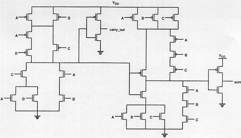
CMOS logic uses complementary pairs of P-type (PMOS) and N-type (NMOS) transistors to implement logic functions. PMOS transistors typically receive input from a voltage source or other PMOS, while NMOS transistors receive input from ground or other NMOS. Advantages include low power consumption, high noise margin, and design simplicity; disadvantages include high input capacitance affecting speed.
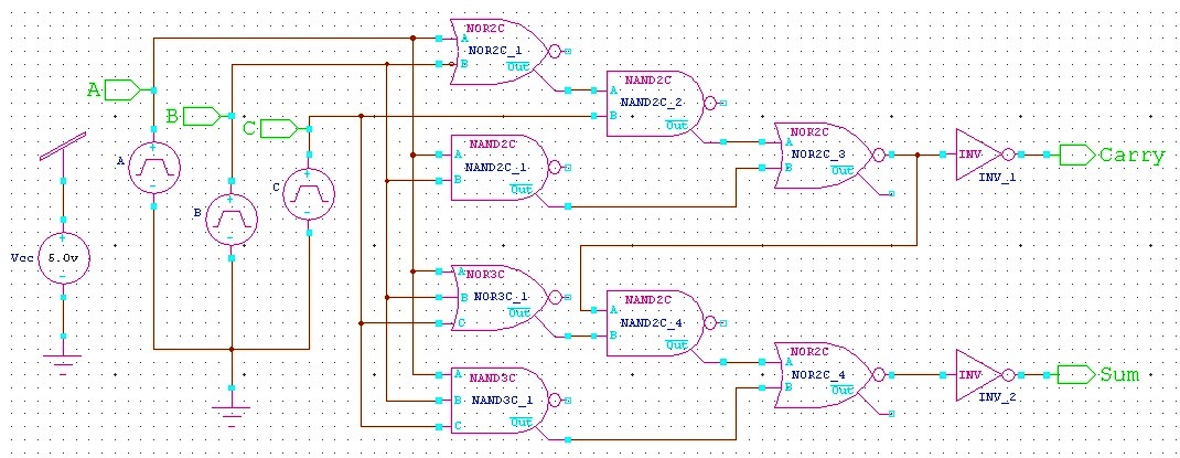
Full Adder Gate-Level Schematic
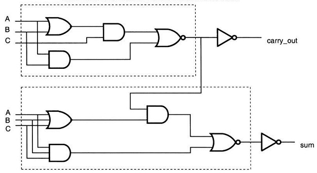
A full-adder has three inputs: A, B, and Carry-in (Cin), and two outputs: Sum and Carry-out (Cout). Boolean expressions:
Sum: Sum = A'B'Cin + A'BCin' + AB'Cin' + ABCin
Carry-out: Cout = AB + ACin + BCin
Full Adder Symbol & Truth Table
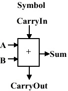
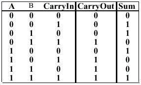
Fig.2: Symbol and Truth Table of Full Adder
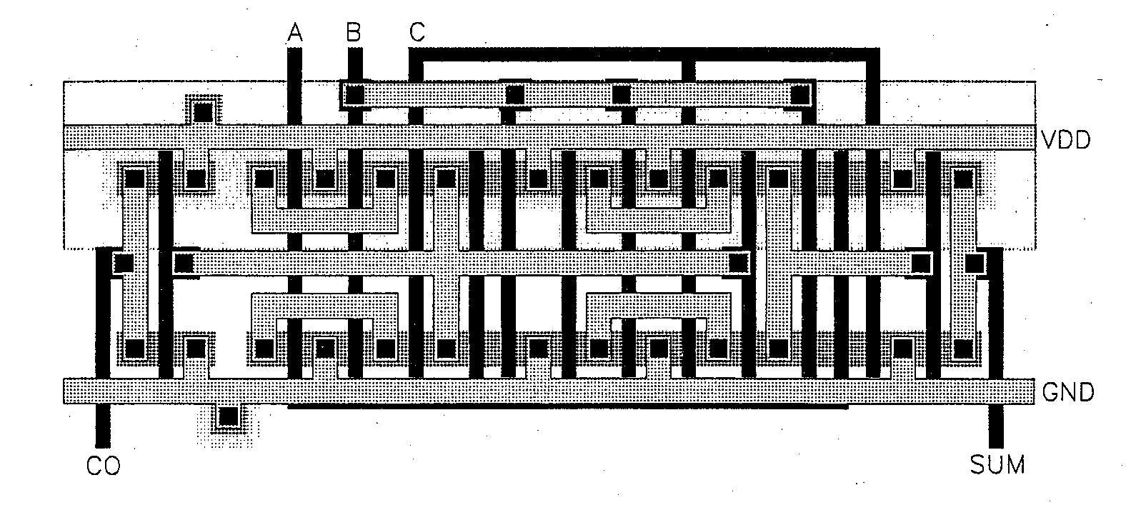
Circuit / Block Diagram
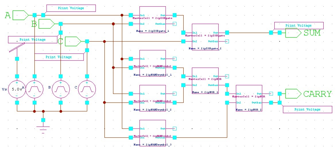
Programming (SPICE Command)
SPICE code is extracted using T-Edit.
Graphs (W-Edit)
Simulate the schematic and generate corresponding waveforms using W-Edit.
Conclusions
The transient response of the CMOS Full Adder was studied. Waveforms were obtained using W-Edit, and SPICE code was extracted using T-Edit. The observed waveforms match the theoretical truth table, validating the design.