Introduction to Tanner EDA Tools


Getting Started with Tanner EDA Tools for IC Design

Introduction to Tanner EDA Tools

Designing modern analog and mixed-signal integrated circuits (ICs) presents numerous challenges, including faster time-to-market requirements, strict cost constraints, and the need for precise verification. To address these challenges, designers rely on comprehensive Electronic Design Automation (EDA) tools. Among the most widely used in industry and academia is the Tanner EDA suite, which provides a complete platform for IC design, simulation, and verification.

Overview of Tanner EDA Suite

The Tanner EDA suite is a collection of interconnected tools that streamline the process of designing integrated circuits. Its key components include:

  • S-Edit: A schematic capture tool for designing circuit diagrams.
  • L-Edit: A layout editor for creating the physical representation of the IC.
  • W-Edit: A waveform viewer to visualize and analyze simulation results.
  • T-Edit: A SPICE simulation engine integrated with S-Edit for verifying circuit behavior.

Why Tanner EDA is Essential

Tanner tools offer several advantages for designers at all levels:

  1. Cost-Effective: Tanner provides a high-performance platform that is affordable for startups and educational institutions, without sacrificing functionality.
  2. Technological Innovation: The suite supports complex and innovative designs, suitable for top-tier companies as well as small enterprises.
  3. PC-Optimized: Fully optimized for Windows PCs, Tanner tools eliminate the need for specialized hardware while maintaining high-speed performance.

Design Workflow and Modules

A typical workflow using Tanner EDA involves several stages:

  • S-Edit: Capture your circuit schematics, defining all components and connections.
  • T-Edit: Perform SPICE simulations directly from the schematic to validate circuit behavior.
  • L-Edit: Develop the physical layout, ensuring proper design rules are followed.
  • LVS & DRC Checks: Verify that your layout matches the schematic and adheres to design rules.
  • W-Edit: Analyze waveform outputs to confirm that simulations meet design specifications.

Visual Examples

Schematic Capture (S-Edit)
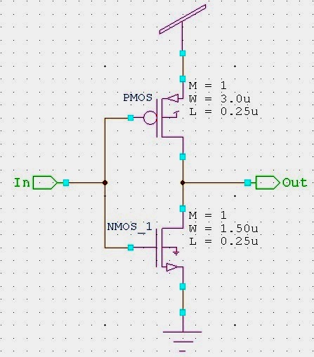
Schematic diagram of CMOS inverter created using Tanner S-Edit
Fig. 1. Schematic of CMOS Inverter

Layout Design (L-Edit)

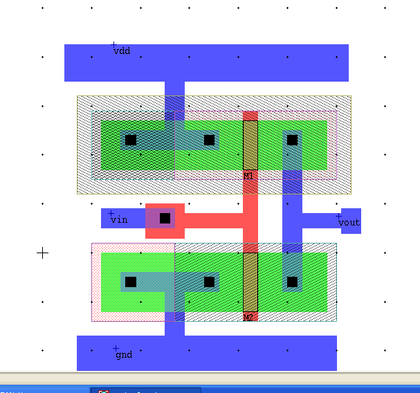
Physical layout of CMOS inverter using Tanner L-Edit
Fig. 2. Layout of CMOS Inverter

Waveform Analysis (W-Edit)

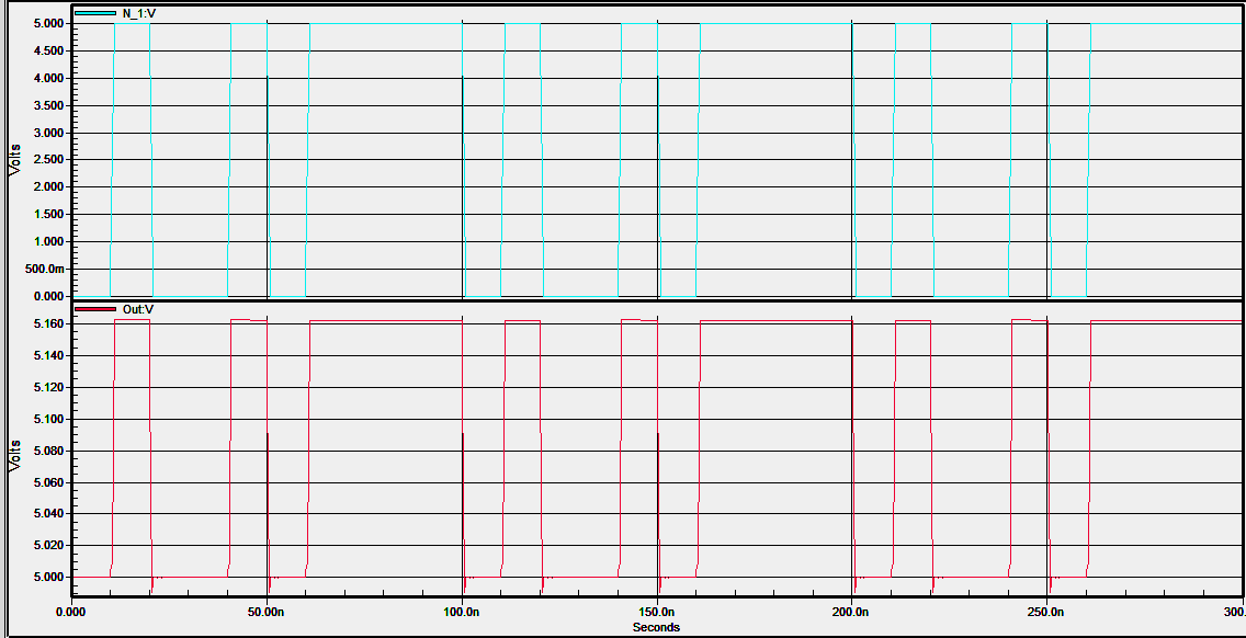
Waveform output of CMOS inverter analyzed in W-Edit
Fig. 3. Waveform of CMOS Inverter

SPICE Simulation (T-Edit)

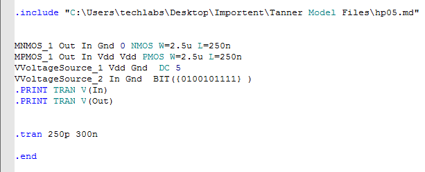
T-Spice simulation results of CMOS inverter
Fig. 4. T-Spice Simulation of CMOS Inverter

Practical Insights

Using Tanner EDA tools allows designers to seamlessly transition from schematic design to physical layout while verifying circuit functionality at each stage. SPICE simulations can include parasitic effects from the layout to ensure realistic performance. This integrated approach reduces errors, accelerates development, and ensures high-quality IC designs.

Summary

  • Integrated tools reduce design errors and save time.
  • SPICE simulation ensures circuit reliability before fabrication.
  • Layout verification via LVS and DRC is critical for functional correctness.
  • Waveform analysis confirms design performance in real conditions.
  • The four generations Integrated Circuits include: 1st Gen (Small-scale integration, SSI), 2nd Gen (Medium-scale integration, MSI), 3rd Gen (Large-scale integration, LSI), and 4th Gen (Very large-scale integration, VLSI).
  • ICs provide compact design, reduced cost, lower power consumption, higher reliability, and faster circuit operation compared to discrete circuits.
  • ICs can be categorized as Analog ICs, Digital ICs, Mixed-Signal ICs, and Application-Specific Integrated Circuits (ASICs).

Understanding Tanner EDA tools equips designers with the skills needed for efficient circuit design, simulation, and verification, making them ready for both academic and professional IC development projects.


Contact Us

Name

Email *

Message *

Popular Posts

Q-function in BER vs SNR Calculation (with Simulation)

Q-function in BER vs. SNR Calculation In digital communications and signal processing, the Q-function plays a significant role in predicting system reliability. It allows engineers to quantify the probability that Gaussian noise will exceed a specific threshold, causing a bit error. What is the Q-function? The Q-function is a mathematical function representing the tail probability of the standard normal (Gaussian) distribution. It is the complementary cumulative distribution function (CCDF) of a standard Gaussian distribution. Q(x) = (1 / √(2Ï€)) ∫â‚“∞ e^(-t² / 2) dt Q-Function Interactive Simulator Move the slider to see how the "Tail Probability" (the area in red) changes. This area represents the Probability of Error (BER) . Threshold Distance ( x ) — (Simulates Increasing SNR) x = 1.0 Q(x) = 0.1587 ...

BER vs SNR for M-ary QAM, M-ary PSK, QPSK, BPSK, ...(MATLAB Code + Simulator)

Bit Error Rate (BER) & SNR Guide Analyze communication system performance with our interactive simulators and MATLAB tools. 📘 Theory 🧮 Simulators 💻 MATLAB Code 📚 Resources BER Definition SNR Formula BER Calculator MATLAB Comparison 📂 Explore M-ary QAM, PSK, and QPSK Topics ▼ 🧮 Constellation Simulator: M-ary QAM 🧮 Constellation Simulator: M-ary PSK 🧮 BER calculation for ASK, FSK, and PSK 🧮 Approaches to BER vs SNR What is Bit Error Rate (BER)? The BER indicates how many corrupted bits are received compared to the total number of bits sent. It is the primary figure of merit f...

Pulse Width Modulation (PWM)

Pulse-width modulation (PWM), or pulse-duration modulation (PDM), is a method of controlling the average power delivered by an electrical signal.   Fig: An example of PWM in an idealized inductor driven by a blue line voltage source modulated as a series of sawtooth pulses, resulting in a red line current in the inductor.    Generating a PWM Signal The simplest way to generate a PWM signal is the intersection method, which requires only a sawtooth or a triangle waveform (easily generated using a simple oscillator) and a comparator. When the value of the reference signal is more than the modulation waveform, the PWM signal (magenta) is in the high state; otherwise, it is in the low state.      Duty cycle A low duty cycle equates to low power because the power is off for most of the time; the word duty cycle reflects the ratio of "on" time to the regular interval or "period" of time. The duty cycle is measured in percent, with 100% representing full o...

Frequency Shift Keying (FSK) Modulation & Demodulation (with Simulation)

Frequency Shift Keying (FSK) Theoretical Foundations: Frequency Shift Keying (FSK) is a discrete frequency modulation scheme wherein the digital information is encoded via instantaneous shifts in the carrier signal's frequency. The fundamental implementation is Binary FSK (BFSK), which maps binary data onto two distinct, discrete spectral states. A binary '1' (the "mark" state) is represented by a carrier frequency \( f_1 \), while a binary '0' (the "space" state) corresponds to frequency \( f_2 \). Each symbol is sustained for a bit interval denoted by \( T_b \). FSK Transmitter Characterization: The mathematical model for the modulated BFSK output \( s(t) \) is defined as: \[ s(t) = \begin{cases} A_c \cos(2\pi f_1 t), & \text{for } m = 1 \\ A_c \cos(2\pi f_2 t), & \text{for } m = 0 \end{cases} \] ...

FFT Butterfly Method Explained (with Example of 4-point DFT)

  FFT Using Butterfly Method Given: x[n] = {0, 1, 2, 3} Step 1: Split into Even & Odd Even indices: x e = {0, 2} Odd indices: x o = {1, 3} Step 2: 2-point DFT For any {a, b}: DFT = {a + b, a - b} Even Part: E = {0+2, 0-2} = {2, -2} Odd Part: O = {1+3, 1-3} = {4, -2} Step 3: Combine Using Butterfly X[k] = E[k] + W k O[k] X[k + N/2] = E[k] - W k O[k] For N = 4: W 0 = 1 W 1 = -j Final Calculations X[0] = 2 + 4 = 6 X[2] = 2 - 4 = -2 X[1] = -2 + (-j)(-2) = -2 + 2j X[3] = -2 - (-j)(-2) = -2 - 2j Final Answer: X[k] = {6, -2 + 2j, -2, -2 - 2j} Try Interactive Online Simulations Interactive FFT Online Simulator (For understanding Fundamentals)  Interactive FFT Online Simulator (Analyze .CSV, .MP3, .MP4, etc. Further Reading Fourier Transform OFDM Return to Fourier Transform Main Page →

Design of CMOS Flip-Flops (SR, D, JK)

Design of CMOS Flip-Flops (SR, D, JK) A flip-flop or latch is a circuit with two stable states, used to store state information. It is the basic storage element in sequential logic and a fundamental building block in digital electronics systems, including computers and communication devices. Flip-flops and latches act as data storage elements for states, pulse counting, and synchronization of variably-timed input signals to a reference clock. Flip-flops can be transparent/opaque (latches) or clocked (synchronous, edge-triggered). Latches are level-sensitive, while flip-flops are edge-sensitive. In sequential logic, the output depends on current inputs and previous states. Fig.1 shows a sequential circuit combining a combinational block and a memory element. ...

AM Modulation Online Simulator

Amplitude Modulation Simulator s AM (t) = A c [1 + k a m(t)] cos(ω c t) where, ω = 2πf & k a = Amplitude Sensitivity Modulation index, μ = k a A m Message Frequency (fm): Carrier Frequency (fc): Carrier Amplitude (Ac): Modulation Index (m = Am / Ac):