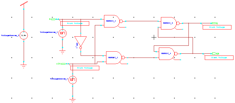
Design of CMOS Flip-Flops (SR, D, JK)


Design of CMOS Flip-Flops (SR, D, JK)

A flip-flop or latch is a circuit with two stable states, used to store state information. It is the basic storage element in sequential logic and a fundamental building block in digital electronics systems, including computers and communication devices.

Flip-flops and latches act as data storage elements for states, pulse counting, and synchronization of variably-timed input signals to a reference clock. Flip-flops can be transparent/opaque (latches) or clocked (synchronous, edge-triggered). Latches are level-sensitive, while flip-flops are edge-sensitive.

In sequential logic, the output depends on current inputs and previous states. Fig.1 shows a sequential circuit combining a combinational block and a memory element.
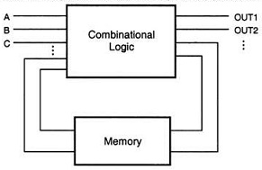
Sequential circuit showing combinational logic block connected to memory element
Fig.1: Sequential circuit consisting of a combinational logic block and a memory
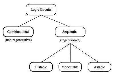
Classification of logic circuits based on temporal behavior
Fig.2: Classification of logic circuits based on temporal behaviour

SR Flip-Flop

The SR latch can be implemented using two NAND gates. The circuit changes state when the Set (S) or Reset (R) input is pulled low. A NAND-based SR latch responds to active-low signals. The truth table and gate-level schematic are shown in Fig.3.
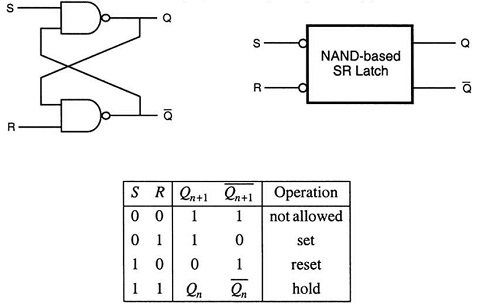
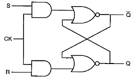
SR latch circuit diagram with block diagram and truth table
Fig.3: Circuit, Block Diagram & Truth Table of SR Latch
SR flip-flop circuit implementation
Fig.4: Circuit of SR Flip-Flop
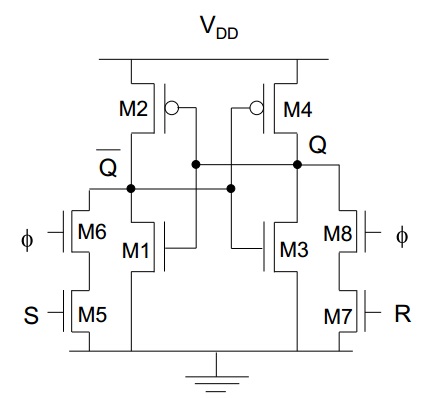
CMOS implementation of SR flip-flop
Fig.5: Circuit of CMOS SR Flip-Flop
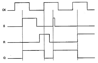
Timing diagram waveform of CMOS SR flip-flop
Fig.6: Timing diagram of CMOS SR Flip-Flop

JK Flip-Flop

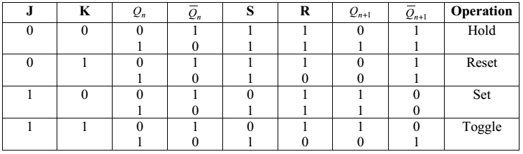
The JK latch solves the "not allowed" input problem of SR latches by using feedback from outputs to inputs. Fig.7 shows an all-NAND JK latch with active-high inputs. J and K correspond to Set and Reset of an SR latch. If both inputs are 1 during the active clock, the latch toggles its state. Table.1 summarizes the JK flip-flop operation.
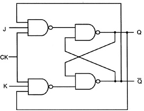
JK flip-flop NAND gate implementation
Fig.7: NAND implementation of the JK Flip-Flop
Truth table of JK flip-flop
Table.1: Truth Table of the JK Flip-Flop
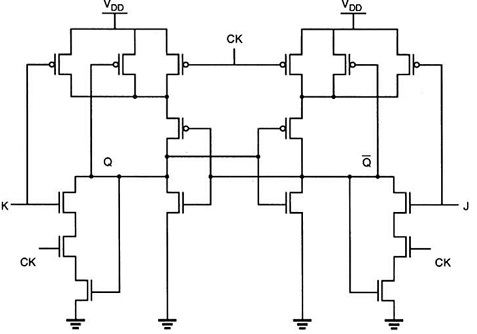
CMOS implementation of JK flip-flop circuit
Fig.8: Circuit of CMOS JK Flip-Flop

D Flip-Flop

The D-latch stores a single logic level and acts as a 1-bit register. It has input D and outputs Q and Q’. It is implemented using a NOR-based SR latch: D connects to S and D’ to R through an inverter. When CLK is high, D is transmitted to Q; when CLK is low, the previous state is retained.
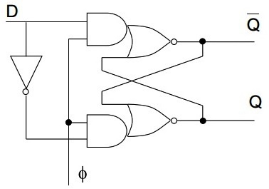
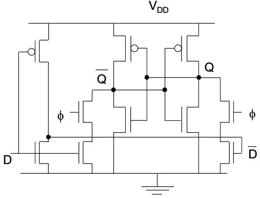
NOR gate implementation of D flip-flop
Fig.9: NOR implementation of the D Flip-Flop
CMOS D flip-flop circuit design
Fig.10: Circuit of CMOS D Flip-Flop

Circuits / Block Diagram using S-Edit
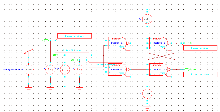
CMOS SR flip-flop schematic using S-Edit
Fig.11: CMOS SR Flip-Flop using S-Edit
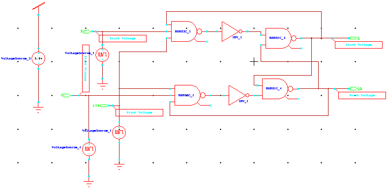
CMOS JK flip-flop schematic using S-Edit
Fig.12: CMOS JK Flip-Flop using S-Edit
CMOS D flip-flop schematic using S-Edit
Fig.13: CMOS D Flip-Flop using S-Edit

Programming (SPICE Command)

Extract SPICE code using T-Edit.

Graphs (W-Edit)

Simulate schematics and generate waveforms using W-Edit.

Conclusions

The transient response of SR, JK, and D Flip-Flops was studied using CMOS logic. Waveforms were obtained using W-Edit, and SPICE code was extracted using T-Edit. Observed waveforms match theoretical truth tables, validating the designs.


Further Reading

  1. Introduction to Tanner EDA Tools
  2. CMOS Logic Gates: Inverter, NAND, and NOR
  3. EDA Tools and VHDL for VLSI Design
  4. Layout of CMOS Inverter
  5. Standard Cell Design in VLSI
  6. Design of CMOS XOR/XNOR Gates
  7. Design of CMOS Full Adder
  8. Design of 8-bit Synchronous Counter
  9. Design of 8-bit Bi-Directional Register
  10. Design of a 12-bit CPU with Basic Instructions
  11. VHDL Logical Function & CMOS Inverter
  12. CMOS Layout Color Codes - IC Design Guide


Contact Us

Name

Email *

Message *

Popular Posts

Q-function in BER vs SNR Calculation (with Simulation)

Q-function in BER vs. SNR Calculation In digital communications and signal processing, the Q-function plays a significant role in predicting system reliability. It allows engineers to quantify the probability that Gaussian noise will exceed a specific threshold, causing a bit error. What is the Q-function? The Q-function is a mathematical function representing the tail probability of the standard normal (Gaussian) distribution. It is the complementary cumulative distribution function (CCDF) of a standard Gaussian distribution. Q(x) = (1 / √(2Ï€)) ∫â‚“∞ e^(-t² / 2) dt Q-Function Interactive Simulator Move the slider to see how the "Tail Probability" (the area in red) changes. This area represents the Probability of Error (BER) . Threshold Distance ( x ) — (Simulates Increasing SNR) x = 1.0 Q(x) = 0.1587 ...

BER vs SNR for M-ary QAM, M-ary PSK, QPSK, BPSK, ...(MATLAB Code + Simulator)

Bit Error Rate (BER) & SNR Guide Analyze communication system performance with our interactive simulators and MATLAB tools. 📘 Theory 🧮 Simulators 💻 MATLAB Code 📚 Resources BER Definition SNR Formula BER Calculator MATLAB Comparison 📂 Explore M-ary QAM, PSK, and QPSK Topics ▼ 🧮 Constellation Simulator: M-ary QAM 🧮 Constellation Simulator: M-ary PSK 🧮 BER calculation for ASK, FSK, and PSK 🧮 Approaches to BER vs SNR What is Bit Error Rate (BER)? The BER indicates how many corrupted bits are received compared to the total number of bits sent. It is the primary figure of merit f...

Pulse Width Modulation (PWM)

Pulse-width modulation (PWM), or pulse-duration modulation (PDM), is a method of controlling the average power delivered by an electrical signal.   Fig: An example of PWM in an idealized inductor driven by a blue line voltage source modulated as a series of sawtooth pulses, resulting in a red line current in the inductor.    Generating a PWM Signal The simplest way to generate a PWM signal is the intersection method, which requires only a sawtooth or a triangle waveform (easily generated using a simple oscillator) and a comparator. When the value of the reference signal is more than the modulation waveform, the PWM signal (magenta) is in the high state; otherwise, it is in the low state.      Duty cycle A low duty cycle equates to low power because the power is off for most of the time; the word duty cycle reflects the ratio of "on" time to the regular interval or "period" of time. The duty cycle is measured in percent, with 100% representing full o...

Frequency Shift Keying (FSK) Modulation & Demodulation (with Simulation)

Frequency Shift Keying (FSK) Theoretical Foundations: Frequency Shift Keying (FSK) is a discrete frequency modulation scheme wherein the digital information is encoded via instantaneous shifts in the carrier signal's frequency. The fundamental implementation is Binary FSK (BFSK), which maps binary data onto two distinct, discrete spectral states. A binary '1' (the "mark" state) is represented by a carrier frequency \( f_1 \), while a binary '0' (the "space" state) corresponds to frequency \( f_2 \). Each symbol is sustained for a bit interval denoted by \( T_b \). FSK Transmitter Characterization: The mathematical model for the modulated BFSK output \( s(t) \) is defined as: \[ s(t) = \begin{cases} A_c \cos(2\pi f_1 t), & \text{for } m = 1 \\ A_c \cos(2\pi f_2 t), & \text{for } m = 0 \end{cases} \] ...

FFT Butterfly Method Explained (with Example of 4-point DFT)

  FFT Using Butterfly Method Given: x[n] = {0, 1, 2, 3} Step 1: Split into Even & Odd Even indices: x e = {0, 2} Odd indices: x o = {1, 3} Step 2: 2-point DFT For any {a, b}: DFT = {a + b, a - b} Even Part: E = {0+2, 0-2} = {2, -2} Odd Part: O = {1+3, 1-3} = {4, -2} Step 3: Combine Using Butterfly X[k] = E[k] + W k O[k] X[k + N/2] = E[k] - W k O[k] For N = 4: W 0 = 1 W 1 = -j Final Calculations X[0] = 2 + 4 = 6 X[2] = 2 - 4 = -2 X[1] = -2 + (-j)(-2) = -2 + 2j X[3] = -2 - (-j)(-2) = -2 - 2j Final Answer: X[k] = {6, -2 + 2j, -2, -2 - 2j} Try Interactive Online Simulations Interactive FFT Online Simulator (For understanding Fundamentals)  Interactive FFT Online Simulator (Analyze .CSV, .MP3, .MP4, etc. Further Reading Fourier Transform OFDM Return to Fourier Transform Main Page →

AM Modulation Online Simulator

Amplitude Modulation Simulator s AM (t) = A c [1 + k a m(t)] cos(ω c t) where, ω = 2πf & k a = Amplitude Sensitivity Modulation index, μ = k a A m Message Frequency (fm): Carrier Frequency (fc): Carrier Amplitude (Ac): Modulation Index (m = Am / Ac):