Layout of CMOS Inverter


Layout of CMOS Inverter

Layout is the process of drawing different mask layers of an IC. Each layer is drawn using a specific color and follows a set of design rules that act as an interface between the designer and the process engineer. Typical considerations include spacing, minimum width, overlap, manufacturability, performance, IC size, and parasitic elements.
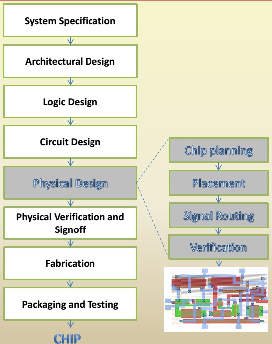
Layout design flow in VLSI
Fig.1. Layout Flow

Design Rules

Design rules are categorized as Lambda (位) rules and Micron rules:

1. Lambda-based rules

  • Scalable rules based on a constant parameter (位).
  • 2位 equals minimum channel length; allows process portability.
  • Processes rarely shrink uniformly, so adjustments may be needed.

2. Micron-based rules

  • Minimum sizes and spacing specified directly in microns.
  • Not tied to 位 multiples; can reduce area by ~50% compared to 位 rules.

Types of design rules include:

  • Intra-layer: Width, spacing
  • Inter-layer: Enclosures, distances, overlaps
  • Specific rules: Antenna, density, minimum area
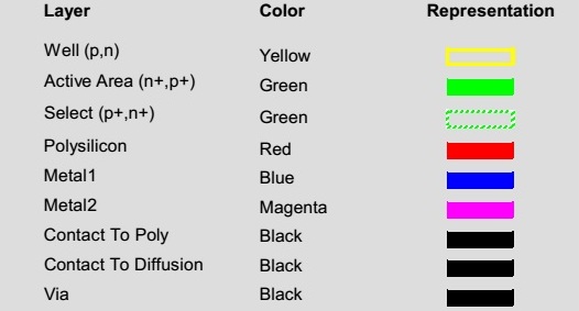
CMOS fabrication process layers
Fig.2. CMOS Process Layers
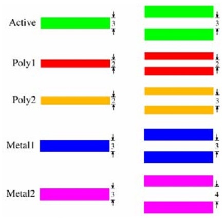
Intra layer design rules illustration
Fig.3. Intra Layer Design Rules

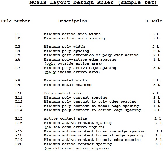
The 位 rules were introduced by Mead and Conway (1980) to allow scalable, portable designs. The MOSIS service provides standard 位-rule sets for academic and commercial designs.
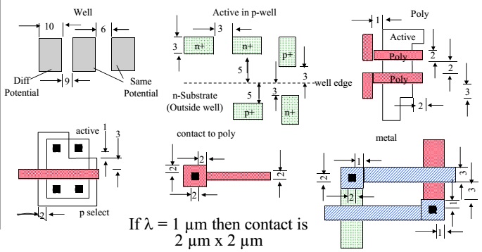
MOSIS lambda based design rules
Fig.4. MOSIS 位-Based Design Rules
Lambda based design rules diagram
Fig.5. Lambda-Based Design Rules

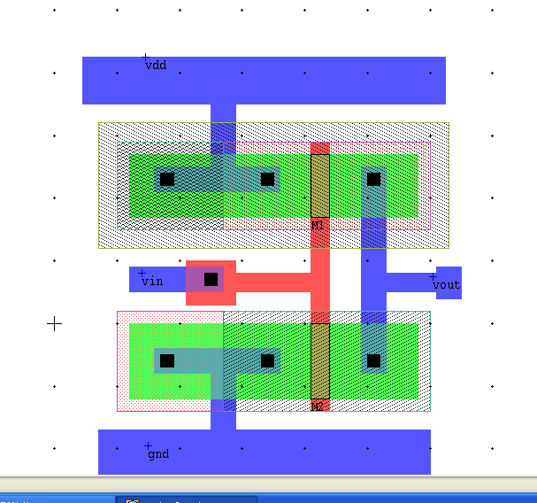
CMOS Inverter Layout

Layout of CMOS inverter in L-Edit
Fig.6. Layout of CMOS Inverter

The layout is drawn in L-Edit following 位 rules and CMOS process layers. After layout generation, it must pass:

  • Design Rule Check (DRC): Automatically verifies that layout polygons follow all design rules.
  • Layout versus Schematic (LVS) check: Ensures the layout matches the original circuit schematic.
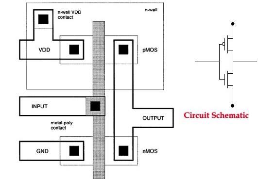
Structure of CMOS inverter layout
Fig.7. Structure of the Layout of CMOS Inverter

Cross-Sectional View

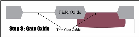
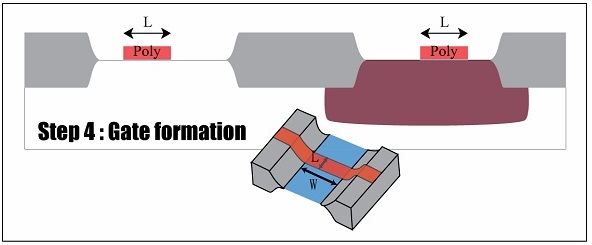
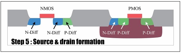
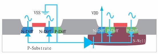
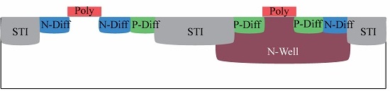
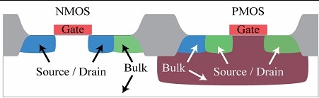
L-Edit allows visualizing the cross-section of the CMOS device, showing the fabrication steps. Observe the drains, sources, gates, and bulks of NMOS and PMOS transistors:
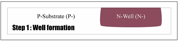
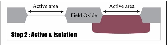
Cross section view step 1 Cross section view step 2 Cross section view step 3 Cross section view step 4 Cross section view step 5 Cross section view step 6 Cross section view step 7 Cross section view step 8

Key observations:

  • Drain and Source are fabricated similarly.
  • All NMOS bulks are connected together.
  • All PMOS bulks in the same N-well are connected together.

SPICE Programming and Graphs

SPICE code can be extracted using T-Edit, and simulations with W-Edit produce the corresponding graphs for verification.

Conclusion

The CMOS Inverter layout drawn using L-Edit was successfully verified using DRC, LVS, and SPICE simulations. The process demonstrated proper adherence to design rules and layout correctness.


Further Reading

  1. Introduction to Tanner EDA Tools
  2. CMOS Logic Gates: Inverter, NAND, and NOR
  3. EDA Tools and VHDL for VLSI Design
  4. Standard Cell Design in VLSI
  5. Design of CMOS XOR/XNOR Gates
  6. Design of CMOS Full Adder
  7. Design of CMOS Flip-Flops (SR, D, JK)
  8. Design of 8-bit Synchronous Counter
  9. Design of 8-bit Bi-Directional Register
  10. Design of a 12-bit CPU with Basic Instructions
  11. VHDL Logical Function & CMOS Inverter
  12. CMOS Layout Color Codes - IC Design Guide


Contact Us

Name

Email *

Message *

Popular Posts

UGC NET Electronic Science Previous Year Question Papers with Solutions

Download Papers and Solutions Exam Pattern Preparation Tips FAQs More Home / Engineering & Other Exams / UGC NET 2026 PYQ 馃搳 Exam Highlights: Electronic Science (88) Feature Details Junior Research Fellowship (JRF) ₹37,000 + HRA per month Eligibility M.Sc/M.Tech in Electronics (55%) Validity of Certificate JRF (3 Years) | Lectureship (Lifetime) 馃摜 Download UGC NET Electronics PDFs Complete collection of previous year question papers, answer keys and explanations for Subject Code 88. Start Downloading 馃搨 View All Question Papers June 2026 - Question Paper Download PDF June 202...

Flat vs Frequency Selective Online Simulator

Flat vs Frequency Selective Online Simulator Channel Type Without Fading Flat Fading Multipaths Nakagami m SNR(dB) Run Simulation Input Signal Signal After Fading Constellation Diagram BER vs SNR Explore Advanced Flat vs Frequency-Selective Fading Simulator Want to see these equations in action? Visualize it. Launch Simulator Tool Flat Fading and Frequency-Selective Fading Effects of Multipath Components and the Nakagami-m Parameter 1. Flat Fading Flat fading occurs when the signal bandwidth is smaller than the channel's coherence bandwidth, meaning that all frequency components of the transmitted signal experience approximately the same fading. It is typically associated with narrowband signals, where the multipath delay spread is small relative to the symbol duration. ...

MATLAB Code for Constellation Diagram of QAM configurations such as 4, 8, 16, 32, 64, 128, and 256-QAM

馃摌 Overview of QAM 馃М 4-QAM MATLAB 馃М 16-QAM MATLAB 馃殌 Online Simulator 馃搨 Other Topics on Constellation Diagrams... ▼ 馃М MATLAB Code for 4-QAM 馃М MATLAB Code for 16-QAM 馃М MATLAB Code for m-ary QAM 馃М Simulator for m-ary PSK 馃М Simulator for m-ary QAM 馃М Overview of Energy per Bit (Eb / N0) 馃М Simulator for ASK, FSK, and PSK Overview of QAM One of the best-performing modulation techniques is QAM [↗] . Here, we modulate the symbols by varying the carrier signal's amplitude and phase in response to the variation in the message signal (or voltage variation). So, we may say that QAM is a combination of phase and amplitude modulation. Additionally, it performs better than ASK or PSK [↗] . In fact, any constellation for any type of modulatio...

UGC NET Electronic Science June 2026 Question Paper with Answer Key & Detailed Solutions

Home / UGC NET PYQ / June 2026 Solved UGC NET Electronic Science June 2026 Question Paper with Answer Key and Full Explanations 馃摜 Download Question Paper (PDF) 2025 2024 2023 2022 2021 2020 Explanations 1. Answer: Option (3) Total Students = 900 Urban Students = 7/10*400 + 4/5*500 = 680 680/900 * 100 = 75.56% 2. Answer: Option (1) Urban Students = 7/10*400 + 4/5*500 + 4/7*700 + 1/2 * 600 = 1380 3. Answer: Option (3) Male = 700*4/7 = 400 Female = 700*3/7=300 400-300=100 100/400*100 = 25% 4. Answer: Option (2) 400*3/10*40/100 + 500*1/5*60/100+700*3/7*50/100+600*1/3*30/100 = 318 5. Answer: Option (2) Total Female Students in B,C, and D colleges = 600 Female Post-graduates  = 100*60/100 + 300*50/100 + 200*30/100 = 270 270/600 *100 = 45% 6. Answer: Option (3) 7. Answer: Option (2) 8. Answer: Option (4) 9. Answer: Option (4) 10. Answer: Option (2) 11. Answer: Option (2) 12. Answer...

Online Simulator for ASK, FSK, and PSK Signal Generation

Interactive Digital Signal Processing (DSP) Tutorial and Simulator for ASK, FSK, and BPSK modulation techniques. Try our new Digital Signal Processing Simulator!   •   Interactive ASK, FSK, and BPSK tools updated for 2025. Start Now Digital Modulation Visualizer: ASK, FSK, & BPSK Simulator Learn and visualize binary modulation techniques (ASK, FSK, BPSK) in real-time with adjustable carrier and sampling parameters. Perfect for DSP students and engineers. 馃摗 ASK Simulator 馃摱 FSK Simulator 馃帤️ BPSK Simulator 馃摎 More Topics ASK Modulator FSK Modulator BPSK Modulator Demodulation More Topics 1. ASK (Ampli...

Design of CMOS Full Adder

Design of CMOS Full Adder VLSI designers historically focus on speed as a key performance metric. High-performance gains are critical for digital processors, microprocessors, DSPs, and ASICs. Small area and high performance are conflicting constraints. Power consumption in CMOS circuits must be minimized to reduce heat dissipation for dense integration and to save energy in battery-powered devices. Power consumption is proportional to switching activity, capacitive loading, and the square of the supply voltage. The Full Adder is a fundamental building block in processors, ALUs, DSPs, microprocessors, and arithmetic operations like addition, subtraction, multiplication, and division. Improving the performance of a 1-bit Full Adder enhances overall system performance. CMOS logic uses complem...

Constellation Diagrams of ASK, PSK, and FSK (with MATLAB Code + Simulator)

Constellation Diagrams: ASK, FSK, and PSK Comprehensive guide to signal space representation, including interactive simulators and MATLAB implementations. 馃摌 Overview 馃М Simulator ⚖️ Theory 馃搱 Q-function 馃摎 Resources BASK Modulation Transmits one of two signals: 0 or $\sqrt{E_b}$, representing binary 0 and 1. Simple but sensitive to noise. BFSK Modulation Transmits one of two signals: $\sqrt{E_b}$ on the Y-axis or $\sqrt{E_b}$ on the X-axis. These are orthogonal signals. BPSK Modulation Transmits $+\sqrt{E_b}$ or $-\sqrt{E_b}$ (antipodal signaling). Most efficient binary scheme. ...